To create a PCB (Printed Circuit Board), I was going to use pre-sensitized material. That is to say that the PCB has a layer of UV sensitive material applied on to of the copper layer. To create a circuit, a transparency of the layout is temporarily fixed on to the board and it is then exposed to Ultra Violet light. Any parts of the board that are exposed become soluble in diluted Sodium Hydroxide* (Caustic Soda) and parts that are covered are less so. The effect is that once the board has been exposed, you can ‘develop’ it. Any of the pattern that is left acts as a resist for the next stage which is etching.
A PCB that has been exposed to UV light through a layout transparency.
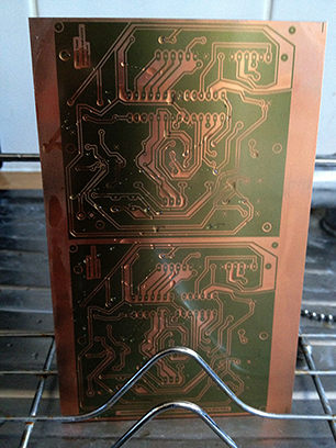
This image is of the first version of the Component/Transistor tester, drying off after having been ‘developed’ in dilute Sodium Hydroxide.
Before I could perform this step, I needed to be able to make an exposure in a safe way. UV Light in concentration can be dangerous so I took that into account. I scouted the internet again and was interested to see several designs that used UV LEDs instead of glass tube bulbs. I found a batch of 100 UV LEDs on eBay and ordered two packs. I then found a likely box and thought about how to create a safe UV Exposure box.
*PLEASE NOTE: Sodium Hydroxide and Ferric Chloride are very dangerous materials and should only be handled by adults and with appropriate safety precautions. Always wear protective gloves and glasses.
You must be logged in to post a comment.